

Osmium deposition technology with CVD method
At Daiwa, we process thin films of osmium by plasma CVD using film formation equipment we developed in-house. (Patented in Japan and United States)
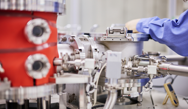
At Daiwa, we apply an osmium coating to the aperture plate that narrows the electron beam. Precious metals such as platinum are sometimes formed on the aperture plates of electron microscopes as an anti-static measure. We propose the use of osmium as a deposition material for this purpose.
Features of Daiwa Techno Systems osmium deposition technology
At Daiwa, we perform osmium deposition on the aperture plates used in electron microscopes.
With electron microscopes, the electron beam can sometimes cause a charging phenomenon. Charging at the aperture plate may prevent the electron beam from being properly narrowed, making it impossible to obtain the desired spatial resolution. Deposition is an effective method to counter this, and one such deposition material is osmium. While platinum deposition is mainly performed by PVD, osmium is deposited by CVD.
The osmium film deposited by the plasma CVD method is a thin film of 10 to 20 nm, which can be formed uniformly up to the inner surface of fine holes. Osmium also has an extremely high melting point (3,045°C) and strong resistance to heat damage. Since the deposition surface is both uniform and extremely smooth, it is suitable for use in a vacuum.
Osmium is a rare blue-gray metal in the platinum group. At 22.57, it has the highest specific gravity of all elements, and has a melting point of 3,045°C, and boiling point of over 5,000°C. Due to its hexagonal close-packed structure, it is stable at both room temperature and atmospheric pressure.
It has an electrical conductivity of 11.4, which is relatively good among rare metals, and has a Mohs hardness of 8, making it an extremely hard metal.
Osmium deposition film thickness
| Film thickness | 10 – 20 nm |